What we can build in Rayong
The process window, equipment and test coverage behind every quote. If your board sits outside a number below, send it anyway: most limits have a special process behind them.
One team from design review to packed product
DFM and layout review
Free before you order: 120+ checks, layout suggestions, and a report within 24 hours of complete files.
Component sourcing
Turnkey purchasing through 860+ partners, with incoming inspection and RoHS and REACH compliant parts.
SMT assembly
Four Yamaha lines with 3D SPI, 10-zone nitrogen reflow, inline AOI and X-ray.
Through-hole
Two lead-free wave lines with pre- and post-wave AOI, plus a hand-solder team. 200,000 joints a day.
Test
First-article inspection, ICT, FCT built to your spec, and burn-in at ambient, high or low temperature.
Coating and box build
Selective conformal coating, depaneling, enclosures, cabling, programming and retail packing.
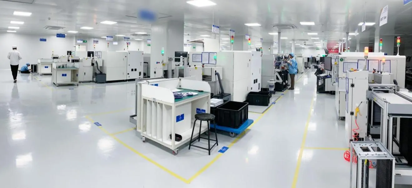
SMT line equipment
- Laser marking for barcodes, QR codes and text on the board
- Automatic board loader and PCB cleaner
- Solder paste management with scan-in, cold storage, warm-up and mixing
- Printer with ±0.018 mm print accuracy, for 01005 and 0.25 mm pitch
- 3D solder paste inspection (SPI) on every board
- Yamaha YRM20 (01005, 72,000 CPH), YSM20R (95,000 CPH, ±0.025 mm) and YSM10 (01005, 0.35 mm BGA)
- 10-zone nitrogen reflow, ±1 °C, with oven temperature monitored and logged to MES
- Inline AOI and X-ray
Through-hole and assembly
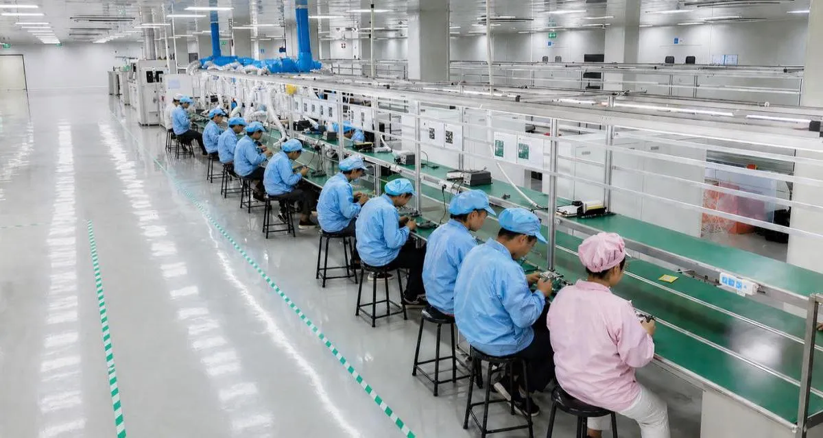
- 3,000 m² ESD-protected through-hole and assembly area
- Pre-wave AOI, automatic flux spraying and 2 lead-free wave solder lines
- Post-wave AOI and a dedicated hand-solder and touch-up team
- Selective conformal coating
- FCT stations built to your test specification
Process window
Standard means routine on our lines. Special means we run it with extra setup or fixtures; ask before you design to it.
| Item | Standard | Special |
|---|---|---|
| Board size | 50×50 to 450×400 mm | Below 50×50, up to 800×450 mm |
| Board thickness | 0.5–3 mm | Below 0.5 or above 3 mm |
| Minimum trace width | 4–6 mil | 1.5–2 mil |
| Layer count | Up to 20 | 24–40 |
| Smallest package | 0201 (0.6×0.3 mm) | 01005 (0.3×0.2 mm) |
| Largest SMD | Up to 200×125 mm | Larger |
| Component height | Up to 15 mm | Above 15 mm; double-sided builds up to 25 mm |
| QFP, SOP, SOJ pin pitch | 0.35 mm | Down to 0.30 mm |
| BGA and CSP ball pitch | 0.35 mm | Down to 0.30 mm |
| FPC | Minimum pin pitch 0.4 mm | |
| Item | Standard | Special |
|---|---|---|
| Board size | 50×50 to 500×400 mm | Below 50 mm, up to 800×400 mm |
| Board thickness | 0.5–5 mm | Below 0.5 or above 5 mm |
| Bottom-side parts | Under 9 mm high; SMT parts kept at least their height + 1.0 mm from through-hole leads | |
| Item | Standard | Special |
|---|---|---|
| CNC routing | Outline tolerance ±0.2 mm (needs a locating fixture) | |
| V-cut | Outline tolerance ±0.5 mm | |
| Coating temperature range | −40 to 120 °C | −50 to 150 °C |
| Coating thickness | 25–50 µm | Above 50 µm (hand applied) |
Inspection and test
Agree the test coverage in writing at quote stage. Every result is stored against the board's serial number.
| Method | What it covers | Throughput |
|---|---|---|
| Smart first-article inspection (2 units) | Chip parts from 01005 up, SOP, QFP and PLCC from 0.3 mm pitch | One part every 5 s |
| 3D X-ray | BGA, QFN and other hidden joints: bridging, voids, offset | 2,000 boards a day |
| ICT (in-house fixtures) | R, L, C, transformers, diodes, transistors, FETs, optocouplers and switching parts | Per program |
| FCT (in-house fixtures) | Every circuit block your test specification calls for, including load and pulse tests | Per program |
| Burn-in | Ambient, high and low temperature | Per program |
Not sure your board fits?
Send the Gerber and BOM. The DFM report tells you what fits, what needs a special process and what to change.